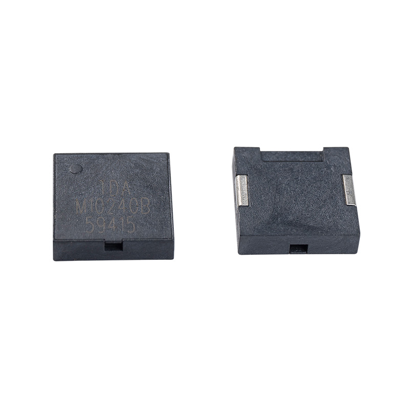
Maximize Acoustic Output with Proper Placement
Placement on the PCB: The placement of the SMD buzzer on the PCB significantly influences its sound output. It should be placed in a location where sound can resonate freely and not be obstructed by other components. Ideally, the buzzer should be placed near the edge of the board to allow sound to escape without interference from surrounding components.
Avoiding Obstructions: Ensure that the area around the buzzer is free of large components that could block or dampen the sound. If possible, place the buzzer on a larger area of the PCB to enhance sound propagation.
Ground Plane and Shielding
Ground Plane: Use a continuous ground plane under the buzzer to reduce the risk of noise and electromagnetic interference (EMI). The ground plane helps provide a stable electrical reference, which is especially important when driving the piezoelectric element inside the passive buzzer.
Shielding: In some cases, electromagnetic interference from surrounding components could affect the buzzer’s performance. Implementing shielding around the buzzer or placing a ground plane near the buzzer can help reduce unwanted interference, ensuring a clean signal for sound production.
Optimizing the Driving Circuit
Decoupling Capacitors: Place decoupling capacitors close to the buzzer's power supply pins to ensure a stable power supply. These capacitors help filter out noise and voltage fluctuations that could degrade the buzzer’s sound quality. Typically, a 0.1µF to 10µF capacitor is used.
Correct Voltage and Impedance Matching: Ensure that the driving circuitry matches the impedance and voltage requirements of the passive buzzer. This might involve using a resistor or transistor to control the current and ensure the buzzer receives the correct voltage levels for optimal sound output.
Driver Placement: Keep the driver circuit (e.g., the oscillator or signal generator) as close to the buzzer as possible to minimize signal loss or delay. The shorter the signal path, the cleaner the audio output.
Signal Routing and Trace Considerations
Short, Wide Traces: Keep the traces leading to the buzzer as short and wide as possible to minimize resistance and signal loss. Longer traces can cause unwanted impedance, signal reflection, or loss of energy that affects the buzzer's performance.
Avoid Signal Crosstalk: When routing the signal traces to the buzzer, ensure they do not run parallel to high-frequency or high-power traces, as this could induce crosstalk or noise that interferes with the sound generation. Keeping signal traces isolated or using ground planes can help prevent this.
Piezoelectric Element Considerations
Optimizing Resonance: The piezoelectric element in an SMD passive buzzer has a natural resonant frequency, and the PCB layout can help enhance or match that frequency. It is important to avoid placing the buzzer near other elements that could cause mechanical damping or vibrations, which would alter the frequency or volume of the sound.
Vibration Control: The PCB design should avoid placing large, heavy components or mounting screws near the buzzer. These could cause vibrations or alter the mechanical properties of the buzzer, leading to distorted sound output. Additionally, ensure the PCB substrate is firm and not prone to vibrations, which could negatively affect sound production.

Thermal Management
Heat Dissipation: Ensure the SMD buzzer does not overheat during operation, as excessive heat can degrade performance or reduce its lifespan. This can be achieved by placing heat-sensitive components away from the buzzer and ensuring there is adequate ventilation or heat dissipation.
Thermal Pads or Vias: If the buzzer’s power consumption is high or if it is part of a larger power circuit, consider using thermal vias or pads to dissipate heat away from the buzzer to prevent overheating and ensure consistent sound performance.
PCB Shape and Enclosure Considerations
Enclosure Design: When designing the PCB, consider the enclosure in which the buzzer will be mounted. The enclosure should allow sound to escape efficiently. A well-designed acoustic enclosure or vent holes near the buzzer can enhance sound output.
Shape of PCB Area Underneath: The area directly under the buzzer should be as open as possible to allow for optimal sound propagation. Avoid placing solid copper or ground planes directly underneath the buzzer, as this can impede sound output.
Minimizing Power Consumption
Optimizing Driver Circuitry: As SMD passive buzzers are used in low-power applications (e.g., battery-powered devices), it’s important to optimize the driving circuitry for low power consumption. Use low-power signal drivers, and consider pulse-width modulation (PWM) or other techniques to reduce the current draw when driving the buzzer.
Efficient Driving Techniques: Some circuits use a resistor in series with the buzzer to limit the current or adjust the volume, which also helps optimize power consumption.
Testing and Validation
Prototype Testing: Always test the layout with a prototype PCB before mass production to ensure that the buzzer performs as expected. Measure the sound output, response time, and efficiency to ensure the layout is optimal.
Simulation Tools: Use PCB simulation software to model the acoustic and electrical characteristics of the buzzer and circuit. This can help detect any potential issues with placement or routing before physical testing.


 EN
EN  English
 Deutsch
 中文简体
中文简体
